

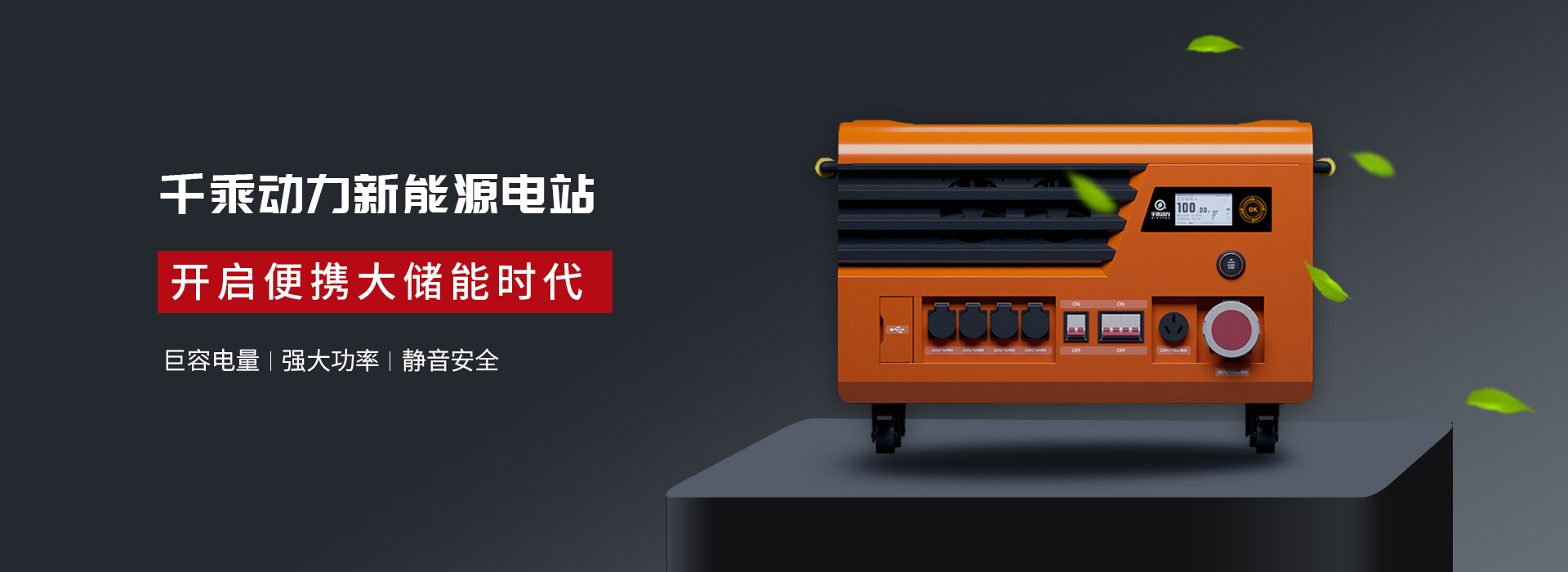
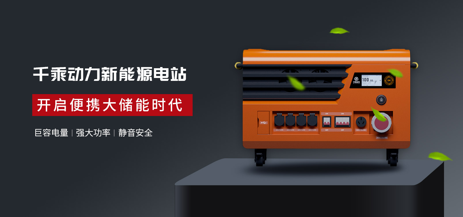
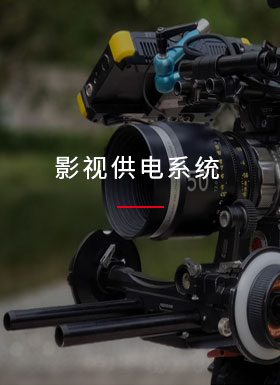
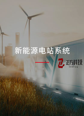
THE MAIN PRODUCTS
产品与服务

融合先进的能源与应用技术,设计友好的服务体系。助力绿色工业与便捷生活,为客户和伙伴创造价值


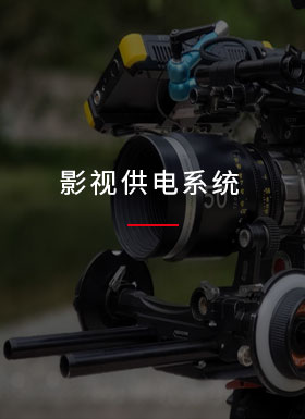
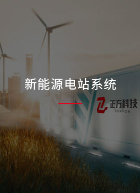
THE MAIN PRODUCTS
产品与服务
融合先进的能源与应用技术,设计友好的服务体系。助力绿色工业与便捷生活,为客户和伙伴创造价值


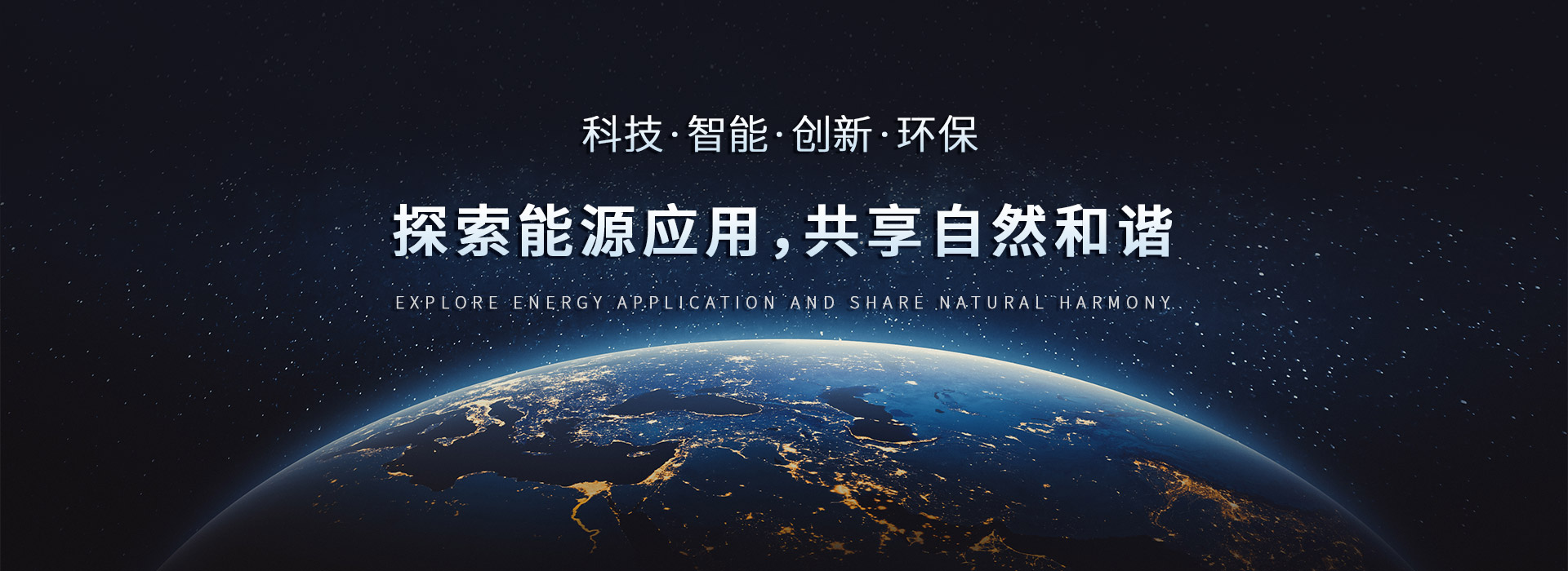
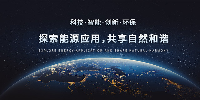
ABOUT US
关于我们
探索能源应用,共享自然和谐
ABOUT US
关于我们
探索能源应用,共享自然和谐
品牌介绍
BRAND INTRODUCTION
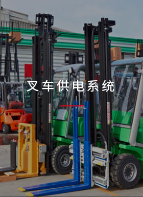
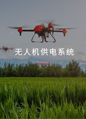
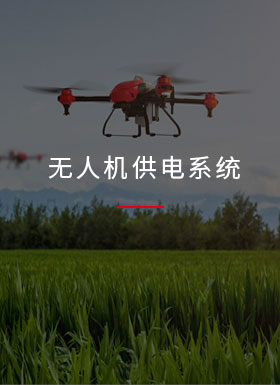
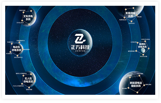
开云app官网入口(中国)有限公司官网创立于2005年,是一家以“智能锂电池模组/锂电池BMS管理系统整体研发、智能制造及销售”的高新技术企业。 公司基于新能源电池智能管理系统(BMS)的研发、设计、智能制造能力,逐渐形成了以叉车供电系统、无人机供电系统、影视供电系统、新能源电站存储管理系统、电动车供电系统、氢燃料供电系统为主的六大业务格局 ……>>


Service advantages
服务优势

无限次免费服务
专业的服务团队,为售前售后提供专业的技术服务, 客服全天候在线,积极响应,为您解决技术问题。

专业技术团队项目化管理
对供应链17年锂电池行业经验技术团队,精益求精,全程项目化、专人、专业无缝对接,保证产品的高品质,高精度。

研发/生产/销售一站式服务
公司基于新能源电池智能管理系统(BMS),以“智能锂电池模组/锂电池BMS管理系统整体研发、智能制造及销售一站式服务。

品牌保证,经验丰富
专注于新能源电池智能管理系统应用,构建共创共享新能源产业数据平台,以技术变革驱动新能源行业的发展。


Service advantages
服务优势
无限次免费服务
专业的服务团队,为售前售后提供专业的技术服务, 客服全天候在线,积极响应,为您解决技术问题。
专业技术团队项目化管理
对供应链17年锂电池行业经验技术团队,精益求精,全程项目化、专人、专业无缝对接,保证产品的高品质,高精度。
研发/生产/销售一站式服务
公司基于新能源电池智能管理系统(BMS),以“智能锂电池模组/锂电池BMS管理系统整体研发、智能制造及销售一站式服务。
品牌保证,经验丰富
专注于新能源电池智能管理系统应用,构建共创共享新能源产业数据平台,以技术变革驱动新能源行业的发展。
CASE CENTER
应用案例
尊重产品,尊重伙伴
CASE CENTER
应用案例
尊重产品,尊重伙伴


NEWS CENTER
新闻动态
专业从事自动智能锂电池模组/锂电池BMS管理系统整体研发、制造及销售
NEWS CENTER
新闻动态
专业从事自动智能锂电池模组/锂电池BMS管理系统整体研发、制造及销售

联系我们
—
网址:www.seven-segments.com
地址: 郑州市高新区金盏街16号亿达科技新城3幢
Emial:zenfon@izeron.com
联系我们
—
网址:www.seven-segments.com
地址: 郑州市高新区金盏街16号亿达科技新城3幢
Emial:zenfon@izeron.com

官方品牌公众号
业务专线:
0371-67992782
客服专线:
177-2979-3469
Copyright © 2018-2020 All Rights Reserved. 豫ICP备2020035352号-1
 客服
客服